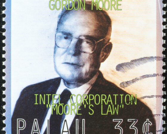
For at least half a century of spectacular advance in semiconductor technology, Intel co-founder Gordon Moore has provided the chip industry with its fundamental productivity benchmark. Year 2015 marked the 50th anniversary of “Moore’s Law”, precisely at a time when many in the semiconductor industry suspected the law was ‘dead,’ or shortly would be.

This was in a situation where the law was often misquoted as being the doubling of the number of transistors on a chip every 12, 18, or 24 months.
In 1965, Gordon Moore started out with a 12-month timeframe and then revised the law in 1975 to a 24-month timeframe. Transistors were not, however, the exclusive reference, and the commonly encountered 18-month reference has been attributed to Intel executive David House, who predicted that chip performance would double every 18 months.
In a 1995 Proceedings Paper published by SPIE (International Society for Optics and Photonics), Gordon Moore explained that, “The original paper that postulated the first version of the ‘law’ was an article I wrote for the 35th anniversary issue of Electronics Magazine in 1965. My assignment was to predict what was going to happen in the semiconductor components industry over the next ten years – to 1975.”
(All following quotes of Moore are from the same SPIE paper)
In 1965, Moore says he calculated, “…the cost of integrated circuits divided by the number of components, a component being a transistor, resistor, diode or capacitor, in an integrated structure at various times. In 1962, the minimum cost per component occurred for circuits containing about ten components.”
Two points arise here. One is that the law was not about transistors per se, but components, including passives. Second, Moore’s “law” was always intimately and intentionally aligned with production cost. The minimum cost was a sweet spot between cost and yield, since “For more complex circuitry, costs skyrocketed because yields collapsed.”
He then predicted that, “the minimum [cost] would continue to go down as we improved out processing capability.” In economic terms, Moore’s “Law” predicted falling component costs, as yields rose.
Based on Micrologic chips from Fairchild, he plotted the number of components in an IC, from 1959 through 1965: “On a semi-log plot, these points fell close to a straight line that doubled the complexity every year up until 1965.”
Then came the projection to 1975: “To make my prediction, I just extrapolated this line another decade in time and predicted a thousand-fold increase in the number of components in at (sic) the most complex circuits available commercially.”
By 1975, Moore was able to demonstrate that the “scatter” of several of the “most complex integrated circuits available commercially from 1965 to 1975” closely coincided with the line. Said Moore, “For a prediction of a thousand-fold increase in complexity, this fits pretty well.”
What drives chip complexity?
Moore then tried to figure out what was driving the annual doubling of components. First, the dice on a silicon wafer were becoming larger as production improved and defect densities fell. Second, the dimensions of the structures on the die were becoming finer – the reduction in device geometries that these days is often called “process shrink”. Observes Moore, “This increases the density on the chip.” And an important technical enabler, here, was the switch to optical lithography, the process whereby interconnects are defined and then etched on the chip.
Moore identified a third factor he called, “circuit and device cleverness,” such as removing space from between components. At this point, Moore realised that while “cleverness” had contributed some 50% of growing chip complexity, this would soon be at an end. There were limits to what cleverness could achieve, and this is what provoked a revision of the law, in 1975, to a doubling of complexity every two years. From then on, complexity would be driven by growth in die size and finer component geometries (process shrinks).
At first, Moore suspected the slowdown in complexity might take as long as five years, but in fact the change came immediately. Moore was then able to calculate that the finer geometries, the decreasing line widths in the integrated circuitry, were the key factor: “…the density contribution from decreasing line widths has stayed almost exactly on the same exponential trend as over the first fifteen year period. If anything, the bias is up, but well within the precision of the data. I think that this is truly a spectacular accomplishment for the industry.”
Soaring production costs
Nevertheless, in 1995 Moore was troubled by rapid increases in production costs, and had personal doubts that his ‘law’ would apply beyond the 0.18-micron node:
“The rising cost of the newer technologies is of great concern. Capital costs are rising far faster than revenue in the industry. We can no longer make up for the increasing cost by improving yields and equipment utilization. Like the “cleverness” term in device complexity disappeared when there was no more room to be clever, there is little room left in manufacturing efficiency.”
This observation continues to haunt the semiconductor industry, as the cost of a new mask set rises above the million-dollar mark and a new fab drives up capex by billions of dollars.
Nevertheless, Moore’s Law has continued to apply through deep sub-micron process nodes and into the nanometer line-width era of today. It is only now that many in the industry doubt whether Moore’s Law will continue to apply at 10 and 7 nanometers and lower. Process complexity is increasing, and with it, design and production timeframes, and expense. One technology that might enable more of Moore, Extreme Ultraviolet (EUV) lithography, has proved a herculean venture in advanced engineering at ASML and elsewhere. Production timeframes have been routinely pushed out. It will probably arrive at some point; the question is “when?”.
Links:
Lithography and the Future of Moore’s Law
Gordon E. Moore, proceedings paper, publ. 19 May, 1995, SPIE Vol. 2438/17
(International Society for Optics and Photonics)
http://www.eng.auburn.edu/~agrawvd/COURSE/E7770_Spr07/READ/1995_SPIE_Speech.pdf
The prediction that chip performance would double every 18 months has been attributed to Intel executive David House:
https://www.cnet.com/news/moores-law-to-roll-on-for-another-decade/
Image: Gordon Moore lecturing in 1970. Photo courtesy of Intel Corp.